

Inseparable From Magic: The Tech Behind ASML
Tiny suns, atomic mirrors, and the bottleneck behind every chip


Hey there 👋
I called TSMC ‘the most important company in the world’ in the title of my recent article here at SK NEXUS.
I called it so because it’s the only company that is manufacturing advanced semiconductors at a speed and precision that’s unmatched in the world.
And also because the two superpowers of our time (US & China) may go to war over that company.
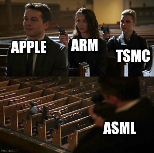
However, it takes a lot of other important companies to make TSMC the most important one. And one of those companies is ASML.
ASML stands for Advanced Semiconductor Materials Lithography and this handful of an acronym simply means that this company does research and manufacture materials for semiconductors manufacturing.
Semiconductors are building blocks of brains of our computers - CPUs, GPUs, etc.
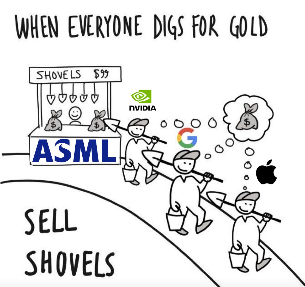
On paper, ASML feels boring. It’s a company based in the Netherlands that sells only a few dozen of its chip-making machines each year to only a handful of companies around the world.
When people talk about AI dominance, they talk about NVIDIA. When people talk about semiconductors, TSMC is the main thing. ASML doesn’t usually make headlines as much as other tech companies do.
Yet it’s one of the most valuable and important tech companies ever to exist not just in Europe but in the world.
For a first time reader, this doesn’t make sense. But if you look a bit closer, everything makes sense.
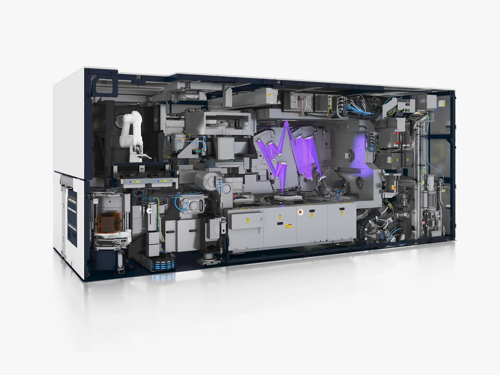
The dozen or so machines that ASML sells each year are their best kept secret.
The EUV (Extreme Ultraviolet) lithography machine as it is called is basically an atomic level printer that prints semiconductor chips.
ASML’s EUV machines are so cool that they’re able to create temperatures hotter than the Sun’s surface, the irony :p
It is a machine that relies on mirrors that take many months to polish and are smoother than physics feels comfortable with.
A machine so complex that replicating it would require rebuilding an ecosystem that took more than 16 countries and 20 years of R&D to produce.
That’s ASML. The only maker of EUV Lithography machines in this world. We have a whole section on EUV lithography machines that we’ll get to shortly.
Because of these EUV Lithography machines, ASML has quietly become one of the most strategically important companies in the world.
The rest of the article would provide a detailed answer as to why that is.
What Does ASML Do?
In our normal discussions whenever we come across the list of important tech companies in the world the answer almost always is a company like Google, Apple, or some other from the silicon valley.
Generally people love to talk about how NVIDIA is the only tech company to reach 5 Trillion dollar market cap but they often forget the companies that are powering the core technology behind the scenes. ASML is one of those companies.
ASML which stands for Advanced Semiconductor Materials Lithography (what a cool name) is a Dutch multinational company that makes the machines used in semi-conductor manufacturing.
Actually, ASML is the only company in the world that makes the Extreme Ultraviolet Lithography machines.
What’s “Lithography”, you might ask?
Lithography is a step in chip manufacturing where patterns are “printed” onto silicon wafers using light. Think of it like an insanely precise projector system.
You shine light through a mask, and that pattern gets transferred onto a photosensitive layer on the wafer.
Smaller patterns mean more transistors. More transistors mean more performance and more efficient chips. And the smaller you go, the harder it gets.
Do that process dozens of times. Stack layers. Add transistors. And you’ve got yourself a semiconductor chip.
Advanced semiconductor chips like those used in our PCs and smartphones are almost all built on ASML’s EUV lithography machines. Without EUV technology, there are no advanced chips to play with.
How Is ASML Different?
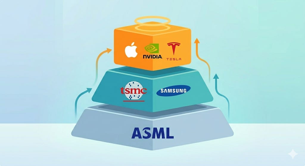
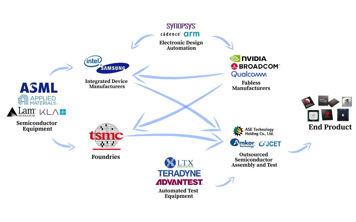
Generally, when you look at companies that are related to semiconductors you can divide them into two categories. These are:
Chip Designers - Companies like Apple, Nvidia are chip designers. They design the hardware specifications of chips. These designers come up with the features of a chip like how many transistors would it have, how much memory would the chip have and so on. These designers don’t physically make the chips.
Chip Manufacturers - TSMC, Intel, Samsung are chip manufacturers. These companies take designs from chip designers and physically manufacture those at scale inside their chip-making facilities. These companies are also known as fabs.
However, ASML is different. It doesn’t fall in either of the above categories. In-fact, it’s in a league of its own.
It is the only company in the entire world that supplies its sophisticated EUV lithography machines to all the chip manufacturers. These machines produce some of the most advanced semiconductor chips.
We’ll go into detail as to why it is the only company making these machines and what’s so special about them. But for now, just know that without ASML’s machines, fabs can’t build out advanced semiconductor chips.
Chip designers can move between fabs. Apple uses TSMC today, but Samsung manufactures for others. Customers can switch partners. Yields improve. Contracts shift.
If you want to make the most advanced chips in the world - 5nm, 3nm, 2nm - there is exactly one place to go for the machine that prints them.
ASML is the only company shipping extreme ultraviolet (EUV) lithography systems at production scale. Without it fabs don’t work and chip designs are useless.
Basically, we won’t have any iPhone launches if ASML suddenly stops existing one fine morning.
The Illegal Tech Behind EUV Lithography
I used the word ‘illegal’ because the technologies behind EUV feel illegal when you try to learn more and dive a bit deeper into their workings.
As a recent article in Financial Times put it, the working of an EUV machine consists of multiple impossible looking processes, all of which have to work 100% of the time at once for the EUV machine to work properly.
Basically, there is zero chance for error and these processes have to be repeated hundreds of times a single second.
Generally, chip manufacturing starts with a silicon wafer - a thin, ultra-flat disc of purified silicon (basically sand).
On that wafer, manufacturers build layer upon layer of circuits. Each layer contains patterns that define transistors, wires, and interconnects.
How do they create those patterns? They use light.....special light.
A light source shines through a mask containing the circuit design. That pattern gets projected onto a photosensitive material. After chemical processing, the pattern is etched into the silicon.
This process is repeated dozens of times.
Smaller patterns mean you can pack more transistors into the same area. That’s basically the infamous Moore’s Law in action.
For decades, chipmakers used deep ultraviolet (DUV) lithography. It worked fine as long as transistors were large enough relative to the wavelength of light being used.
Then we started hitting the limits of Physics because features of our chips started becoming smaller than the wavelength of light.
This means natural effects like diffraction started distorting the patterns that would be etched onto the silicon wafer.
And once you go that small you can’t just “focus harder.” You start hitting fundamental optical limits.
Engineers tried tricks. Multiple patterning. Complex processing steps. But costs ballooned and complexity just increased and increased.
That’s when EUV entered the scene which isn’t just an upgrade but a totally different universe. And producing the EUV light isn’t just hard. It’s borderline insane.
As someone who’s into science and technology, the technology behind EUV lithography just boggles my mind.
Producing the Extreme Ultraviolet Light
The process of EUV lithography starts with a special kind of light that is artificially produced by us humans. And it took us about 20 years of R&D just to get this light to a usable state in lithography.
EUV stands for Extreme Ultraviolet. It is a special kind of light that is produced through a complex process by ASML. This light is special because it has a wavelength in nanometers and that’s the only light today that allows us to build advanced chips.
To generate that light, ASML’s EUV machine fires powerful lasers at microscopic droplets of molten tin that are ~30 microns in size or about the size of a white blood cell in our bloodstream.
Each droplet is shot at the speed of 250 km/h and the machine’s goal is to shoot a laser on that droplet and convert each droplet into plasma.
That plasma reaches temperatures of about ~219,700 degree celsius or roughly 40 times hotter than the surface of the sun. And as a result of that explosion, EUV light is emitted.
Each tin droplet gets hit 3 times in 20 microseconds in a row. The first shot flattens the tin and the others vaporize it into plasma form. The last shots, then vaporize the metal into plasma.
Just pause for a second and read all of this again. The process of producing that EUV light is a man-made collision between a metal and a laser to create plasma hotter than the surface of the sun just to produce that EUV light.
If you’ve watched the recent movie Oppenheimer it opens with a quote that sits well in the EUV context too:
“Prometheus stole fire from the gods and gave it to man. For this, he was chained to a rock and tortured for eternity”
We are literally shooting lasers at molten metal 50,000 times in a single second to create mini suns inside a man-made machine, just so we can etch tiny lines onto silicon.
And it has to happen continuously, reliably, inside a factory running 24/7, no breaks, no downtime, no nothing!
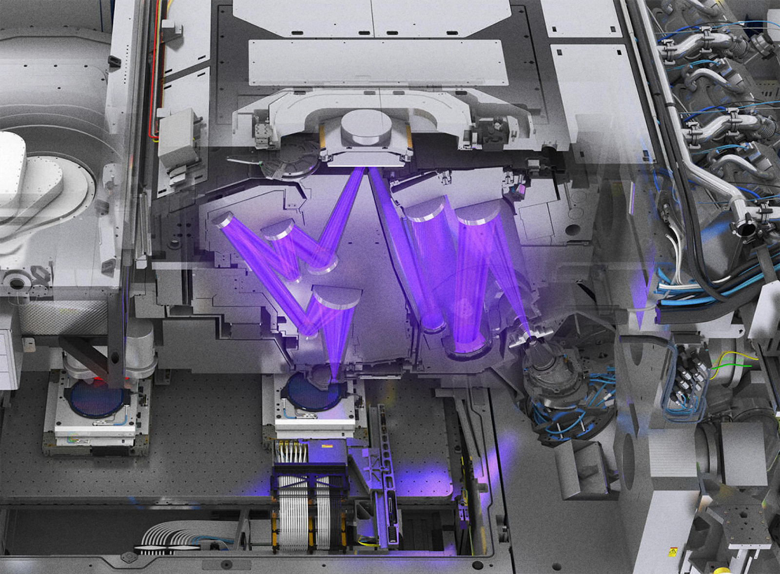
Photolithography and Mirrors
The first job of ASML’s EUV lithography machines is producing the EUV light but that is only half the job because now we need to essentially print using that light, that’s where some special mirrors come in.
Photolithography is the process of getting the EUV light to travel so that it lands on the chip mask (that has the chip architecture), and then onto the final silicon wafer.
And by far, this process is a harder process because of the increasing number of layers and the ever smallest margins of error involved here.
So, now we have the EUV light and the machine now has to reflect that light using a series of the most polished mirrors in human existence to a reticle/mask.
A final semiconductor chip could have 10-100 layers and reticle is basically a mask that has the actual design of layers of a chip. The reticle is so precise that the design is precise up to nanometers, equal to one thousand millionth of a meter.
But things aren’t that simpler because EUV light cannot pass through glass.
That means we cannot use traditional lenses for this light. Instead, the entire optical system that moves EUV to reticle uses mirrors and not just ordinary mirrors.
These mirrors must be polished to atomic-level smoothness. Any defect larger than a few atoms can distort the pattern.
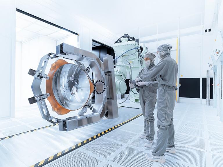
The mirrors are manufactured by Zeiss, a German optics company that has worked with ASML for decades and builds these specialized mirrors that can precisely reflect EUV light.
Components like these mirrors couldn’t be bought off the shelf. They were co-developed through long-term research partnerships, funded across years and billions of euros.
Each mirror contains multilayer coatings designed specifically to reflect EUV at 13.5 nm.
Even then, they only reflect about 70% of the light. After multiple reflections, only a fraction of the original EUV intensity (about 4%) remains.
And that is used by the reticle to print a chip layer and when we stack hundreds of those layers precisely on the final wafer, we get an advanced semiconductor that powers our iPhones, GPUs and self-driving cars.
The Machine Itself
Now let’s zoom out a bit and talk about the EUV lithography machine as a whole.
According to Wired, an EUV machine contains over 100,000 parts. It weighs more than 180 tons and requires specialized vacuum chambers because EUV light gets absorbed by air.
The machine also needs hyper-specialized vibration isolation so precise that even small tremors could ruin the patterning process. They say if a human even leans on an EUV machine the production gets affected.
The wafer stage moves at high speeds but must position wafers with nanometer precision, less than the width of a few atoms.
Everything must align perfectly too. If the laser timing is off and it doesn’t shoot the tin, the plasma fails.
If the mirrors drift, the pattern on our reticle distorts. If vibrations leak in, production gets spoiled and final yield gets affected.
Every step is almost impossible. And all of them must work at the same time.
That’s the TECHNOLOGIA for you :p
Why No One Has Copied ASML (Yet)?
It’s not that no one has tried to copy ASML but no one has succeeded in doing that. Japanese companies like Canon, Nikon jumped on the EUV train but went sideways.
The combination of ASML’s decades of operations that included DUV and now EUV lithography means it has the data advantage that no other company in the world has.
It’s the only company that has not placed a bet on EUV but has made it a success because its machines run 24/7 in fabs like Samsung, TSMC, Intel.
Real world data from having that many machines running for that much time gives ASML the advantage that no competitor has.
Still there are multiple reasons behind ASML’s domination of the EUV technology. Below, I’ll break down some of them:
The Complex Supply Chain
ASML’s final EUV lithography machine that ASML sells has more than 100,000 parts. And the majority of those parts are specially engineered for these specific machines.
A normal supply chain cannot provide lasers that could turn tin to plasma nor mirrors that take months to just polish. This is a multi-decade technological alliance.
At this point you must be thinking:
“Okay, it’s hard. But Uncle Sam (US government) has almost infinite money. Why don’t they have their ASML?”
The thing is that ASML didn’t build EUV alone.
The development of EUV took more than two decades and cost billions of euros. At one point, Intel, TSMC, and Samsung themselves invested directly into ASML to accelerate development because they just needed to ship more chips.
Companies like TSMC and Samsung funded ASML’s research because they were the biggest benefactors of EUV lithography machines. They had iPhones and Samsung Galaxy to sell each year and the demand for chips has only increased.
In other words, the industry funded the monopoly.
But why? you may ask:
Because the alternative - each company trying to build its own EUV ecosystem was even more expensive and slower. ASML was the only one that had a stellar track record for chip-making machines.
Another reason for ASML’s monopoly position is the supplier lock-in. The company’s supply chain is also limited to quite a few companies in the region.
For example: Zeiss (Germany) builds the mirrors that take months to just polish. Trumpf (German Company) provides those high-power lasers that turn metal into sun surface temperatures.
Specialized components used in the final EUV machine also come from highly niche suppliers scattered mostly across Europe, which gives ASML a regional supplier trust.
If other companies wanted to build EUV lithography machines they first had to rebuild this entire network of component companies from scratch.
This means they first have to reverse engineer most of those specialized components.
Rebuilding that network from scratch isn’t just expensive. It’s an insane challenge from a practical POV because it took decades for ASML to build that network.
Even the United States, despite giving away billions of dollars through their massive CHIPS Act funding, does not currently have an ASML EUV alternative.
China has been trying to develop advanced lithography tools, but remains years behind in EUV capability
More than the capital, it’s about time, and accumulated experience in R&D and production for decades that is ASML’s moat.
The Very Long Term Economics
Even if someone could copy ASML’s technology, it’s hard to justify from a money and common-sense perspective.
We know that each EUV machine reportedly costs over $150 million and only a handful of companies in the world can afford them. TSMC, Samsung, Intel are some of them.
That means your customer base is tiny but really demanding too. Just TSMC alone powers NVIDIA, Apple, Tesla, and so on.
If you’re a new entrant to EUV lithography market, you’d need:
Decades of R&D
A working global supplier ecosystem
Customers willing to trust your unproven system
All while competing against a company that already has spent decades in R&D, built a stable supplier ecosystem and handles some of the most sophisticated chips we’ve ever produced.
In lithography companies like NVIDIA, Apple cannot take risks. If your machine fails for a day, billions in wafers are wasted right away.
That’s why no one wants to be the beta tester because their customers and especially the demand because of AI just doesn’t allow them to take risks.
So even if someone built a technically comparable tool, convincing TSMC to switch would be a mountain of effort entirely.
Geopolitics Enter the Chat
It looks like it’s impossible to remove politics when there are humans involved. Lithography is no different.
ASML sits in the Netherlands. The Dutch government, under pressure from the US, has restricted exports of advanced EUV systems to China. They simply cannot sell EUV lithography machines to the biggest manufacturer in the world.
That means ASML’s machines aren’t just industrial equipment. They are geopolitical leverage. Trump’s pressure works on the company because the US has contributed a lot of R&D effort along with many billions to get EUV lithography working.
Controlling advanced lithography means controlling advanced chip production which goes into Artificial Intelligence, iPhones and Self-driving cars.
The US has been pretty vocal in maintaining a lead in AI over China. They call it a matter of national security and ASML is one of their levers to protect their sovereignty over the AI infrastructure.
What Does The Future Look Like?
Because of the Artificial Intelligence boom, we’re going through a wave of demand that we’ve never experienced in the history of computing ever before.
NVIDIA wants to sell more GPUs because OpenAI just can’t get enough of them. Apple’s new iPhone launches get sold more and more and Tesla needs more chips to drive their self-driving computer system.
Although this unusual demand has been bad for us consumers in the form of scarce GPUs and 4x prices of RAM in a matter of months, it is also pushing R&D to further enhance EUV’s potential.
That’s why a couple of days ago ASML reported a breakthrough in EUV tech. Their tin firing lasers have now become more powerful which means the laser can fire 100,000 tin droplets every second (going from a previous rate of 50,000/second).
This means the production capacity would gradually speed up straight up by 50% and the company plans to implement this by 2030.
Other than ASML, China has also heated up its efforts of reverse-engineering ASML’s EUV lithography machines. It is widely known that China has been dumping billions for more than a decade to achieve chip independence.
A couple of months ago, news broke out that China has successfully hacked ASML’s EUV technology. While it’s possible that China could reverse engineer parts of the EUV tech chain, the country has yet to ship chips based on their machines.
This unusually high demand of semiconductors is pushing ASML to innovate more and further optimize its processes.
China and the US are pushing more towards chip independence, especially in the wake of concerns that China may overtake Taiwan by force because of TSMC.
If you’re not sure why China may start World War 3 over a small country because of TSMC, you should check this article on the company that is at the heart of this issue.
ASML is already working on Next-generation lithography processes that sound science-fiction to someone like me. Here’s what the company is working on:
X-ray lithography
Electron beam lithography
Quantum lithography
I’d have loved to talk about the next-gen lithography technologies that ASML is working on but I feel we’re out of space for this article.
This article is already quite short to fully discuss ASML’s current EUV technology, let alone even briefly discuss the next generation tech they’re working on.
Maybe someday we may discuss some of their newer technologies mentioned above. If you’re excited for that, let me know in the comments and I’ll start working on that too :)
Out of all articles I’ve written for SK NEXUS, this was by far the one which involved the most research. My main challenge was to balance the theoretical physics concepts and the practical chip-making processes into a ~3500 words piece.
And in all of this I had to make sure that I’m not making it boring or using terms our Bashir doesn’t know about.
Still, I enjoyed it more than the other articles because of my personal interest in the topic. I hope your eyes glitter the same way mine have done while writing this piece.
And I would love to listen to your thoughts in the comments. I read all of the comments and any kind of feedback is welcome. If you found this blog helpful in any way, a comment or a share would make my day.


Great breakdown of the EUV moat, the physics are genuinely staggering. One thing worth layering on from an investor's standpoint: ASML doesn't just have a product monopoly, it has a timing monopoly. Equipment orders tend to lead chip fab demand by 12–18 months, which means ASML's backlog and order intake are arguably the best leading indicators in the entire semiconductor supply chain, more forward-looking than TSMC's quarterly guidance or Nvidia's unit demand. The recent EUV throughput breakthrough (tin laser firing rate doubling to 100K droplets/second by 2030) is actually a capacity expansion story, not just a tech story. The question I'd push back on slightly: with ~$35B in backlog as of late 2025 and EUV shipments tightly rationed, does ASML's pricing power get tested if fab capex cycles soften before 2027? Or is the backlog deep enough to insulate them?