



Hey there 👋
You might know that countries, especially the US and China, are trying their best to bring chip manufacturing back to them.
TSMC’s Arizona fab is already printing out advanced chips for the likes of Apple and NVIDIA, with 3nm production planned there for 2027-28.
All of that is interesting and exciting but none of that makes sense unless you understand how chips actually get made.
The weird fact is that the processor in your phone, the GPU in your gaming PC and the chip in your car’s computer, they all started as sand on a beach somewhere.
Literal sand. The stuff you walk on. The stuff kids build castles with.
The question is how do you go from literal sand to a complex chip with billions of transistors, where a single transistor is about tens of thousands of times smaller than a human hair.
The answer is a process so complex and expensive that only a handful of companies in the world can actually do it at scale. You can count these companies on one hand.
This is the first article in a Series where we will cover chip manufacturing from sand to the device in your hand.
As you may have figured out, chip manufacturing is one of the most complex processes in human history. There is simply a lot of maths and physics involved.
However, in this Series, I’ll keep most of the stuff relatively simple for you guys while talking about the important stuff.
One quick side track -
Just so you know, SK NEXUS recently went paid. Linked here is the detailed post by Saqib Tahir that goes into the specifics of it all.
To keep it short, here’s what to expect moving forward:
Our 3-part article Series is going paid. Readers will have to pay a small amount to access our Series.
However, first part of a Series (like the one you’re reading) will be free for all.
Money wasn’t the motivator for going paid. We want quality tech writing to be accessible for most.
That’s why the first part of a Series will remain free, while other parts will be exclusive to those who pay.
If you have any thoughts, please share your feedback down in the comments.
Silicon Is Everywhere But Pure Silicon Is Rare
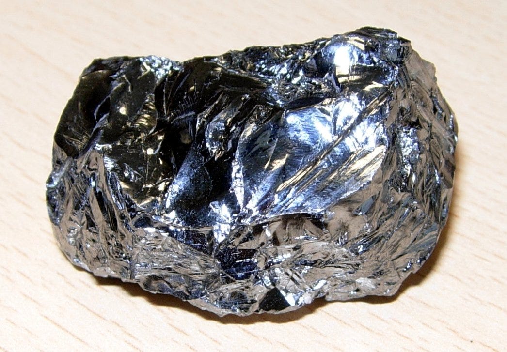
Silicon is the second most abundant element in Earth’s crust after oxygen. It is everywhere.
Rocks, sand, dirt, glass. All of it contains some form of silicon in them.
But here is the thing. Silicon almost never exists alone in nature. It is always bonded to other elements, usually oxygen.
When silicon bonds with oxygen you get silicon dioxide. That is what sand is. That is what quartz is. That is what most rocks are made of.
The silicon we need for chips is not silicon dioxide. It is pure silicon. Just silicon atoms and nothing else.
Getting pure silicon from sand is like trying to extract gold from seawater. Technically possible but incredibly difficult and expensive.
The purity required for chips is absurd. We are talking 99.9999999 percent pure silicon. Nine nines!
One impurity atom for every billion silicon atoms. That is the standard.
Anything less and the chip does not work properly. Transistors fail and there’s a short circuit.
So the entire chip industry is built on a process that takes one of the most common materials on Earth and refines it into one of the purest substances humans have ever created.
What Makes Silicon Special for Electronics
You might be wondering why we use silicon at all. There are other materials. Why not use something easier to work with?
The answer is that silicon has a unique set of properties that make it perfect for electronics.
First, silicon is a semiconductor (Now you know why we call them semiconductor chips).
Being a semiconductor means it can conduct electricity sometimes and block it other times depending on how you treat it.
Metals like copper conduct electricity all the time. Insulators like rubber block electricity all the time. Silicon sits in the middle.
You can control whether silicon conducts or blocks by adding tiny amounts of other elements to it. This process is called doping and we will cover it in a later article.
Silicon’s ability to switch between conducting and insulating states is what makes transistors work. Transistors are the building blocks of every chip and we’ll go over them in detail too in a later article in this Series.
Second, silicon forms a stable oxide layer when exposed to air. That oxide layer is silicon dioxide which is basically glass.
This matters because you can grow extremely thin, extremely uniform layers of silicon dioxide on top of silicon. These layers act as insulators between different parts of the chip.
Third, silicon is abundant and relatively cheap to source. You can find silicon dioxide anywhere on Earth.
Fourth, we have spent 70 years learning how to work with silicon. The entire manufacturing infrastructure is built around it.
There are other semiconductor materials like gallium arsenide or silicon carbide. Some are faster and even more efficient than silicon.
But none of them have the combination of properties, manufacturing knowledge, and cost-effectiveness that silicon has.
That is why every major chip in your life uses silicon. Your phone, your laptop, your car, your router, all silicon.
Making Pure Silicon from Quartz
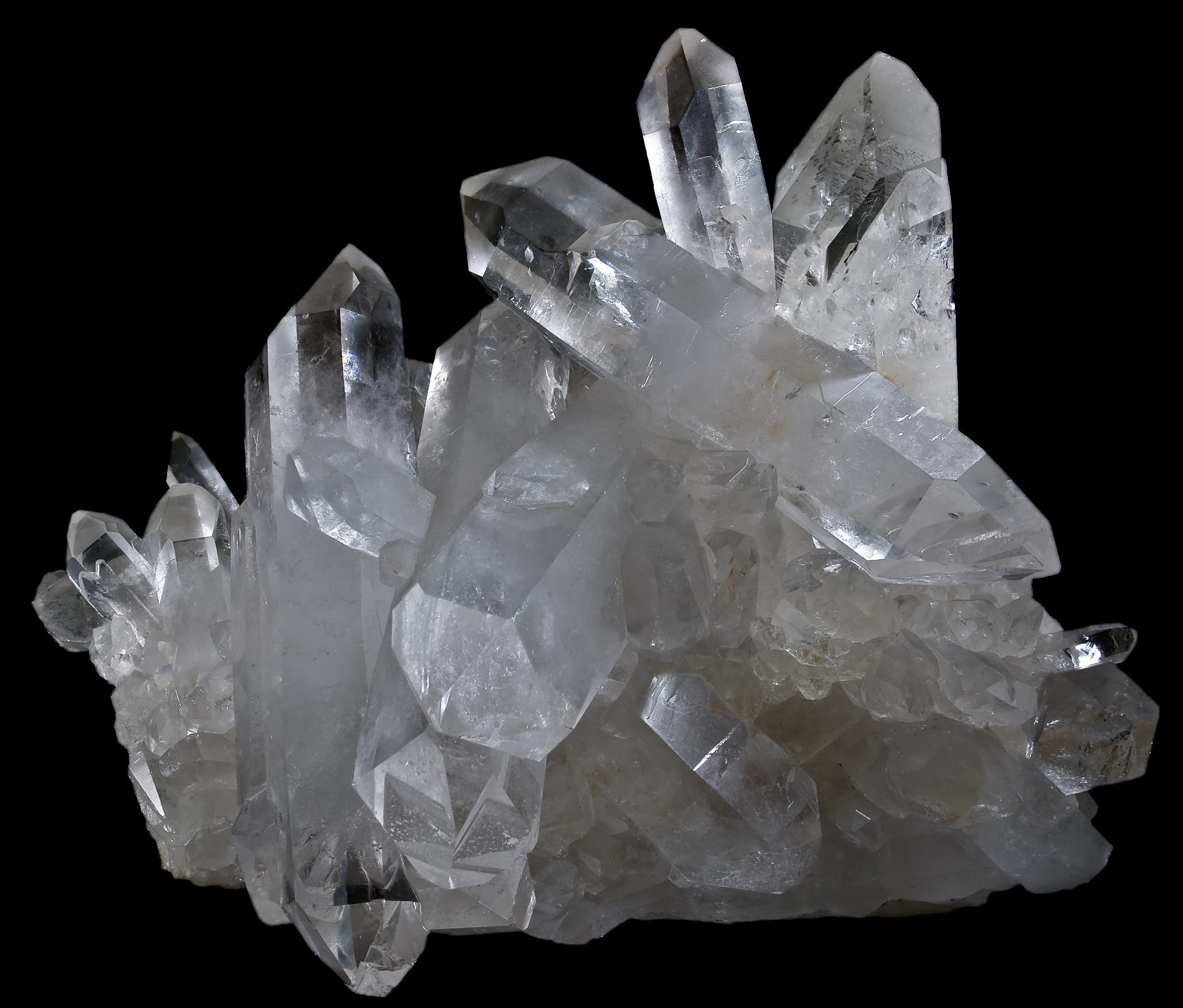
We know that we need pure silicon to make chips and in its natural form silicon is bonded with oxygen and we need to remove that bond and extract pure silicon.
That journey starts with quartzite (aka quartz for short). It is a type of rock that is almost pure silicon dioxide.
Mining companies dig up quartz from a mine. They crush it into smaller chunks. Then they load it into massive electric furnaces to melt it.
Inside the furnace the quartz gets heated to over 2000 degrees Celsius (Yup, furnaces are that hot!). Carbon in the form of coal also gets added to the mix.
At those temperatures a chemical reaction happens. The carbon pulls oxygen away from the silicon dioxide leaving behind molten silicon and carbon dioxide gas.
What comes out is called metallurgical-grade silicon or MG-silicon. It is about 98 to 99 percent pure.
That sounds pretty pure. But for electronics it is nowhere near good enough. MG-silicon is fine for making aluminum alloys or solar panels.
But semiconductor chips are much more demanding. They need something far more pure.
The impurities in MG-silicon include things like iron, aluminum, calcium, and other metals. Even at 1 or 2 percent contamination that is billions of unwanted atoms.
Those impurities will ruin a chip. So the next step is to purify the silicon even further.
Getting to 99.9999999% Purity
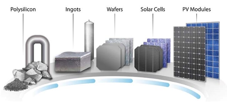
The industry standard for purifying silicon is called the Siemens process. It was developed in the 1950s and we still use it today because nothing better has been invented.
This is also where things get extra expensive. Here is how we purify silicon further:
You take metallurgical-grade silicon and grind it into powder. Then you react that powder with a special acid to produce a chemical compound that is liquid at room temperature.
If you’re curious, that compound is called Trichlorosilane.
Trichlorosilane can be distilled. Distillation is a purification process where you heat a liquid until it evaporates, then cool the vapor back into liquid.
Impurities have different boiling points than trichlorosilane. So when you distill it multiple times the impurities get left behind.
After enough distillation cycles you end up with ultra-pure trichlorosilane and that’s where things get more and more expensive.
You take thin rods of already-pure silicon and place them inside a reactor chamber. Then you pump ultra-pure trichlorosilane gas into the chamber.
The rods get heated to over 1000 degrees Celsius. At that temperature the trichlorosilane gas decomposes and deposits pure silicon onto the rods.
Layer by layer, atom by atom, the rods grow thicker as silicon builds up on their surface.
This process runs for days. The rods slowly grow from pencil-thin to telephone-pole-thick.
When the process finishes you have polycrystalline silicon rods that are 99.9999999 percent pure. Nine nines.
This is called polysilicon or poly-Si. This is what the chip industry uses.
The Siemens process is slow and energy-intensive. It takes enormous amounts of electricity to run those reactors for days on end.
That is why polysilicon is expensive. And that is why companies that make polysilicon are critical to the entire chip supply chain.
Most of the world’s polysilicon comes from a handful of companies in China, Germany, and the United States.
Making the Silicon Ingot
Polysilicon is pure but it is not in the right form still. Chips need single-crystal silicon not polycrystalline silicon.
The difference is in how the atoms are arranged. In polycrystalline silicon the atoms are arranged in small random crystals all jumbled together.
In single-crystal silicon all the atoms line up in one perfect crystal structure.
Single-crystal silicon has better electrical properties. Transistors work more reliably and the overall chip performance is more predictable.
So the next step is to turn polysilicon into a single crystal. The process used is called the Czochralski method or CZ method.
Here is how it works.
You take chunks of polysilicon and melt them in a crucible at over 1400 degrees Celsius. The silicon turns into a liquid pool.
Then you take a small seed crystal of silicon, a tiny piece that already has the perfect crystal structure, and dip it into the molten silicon.
The seed crystal acts as a template. As you slowly pull it up out of the liquid, silicon atoms from the melt attach to the seed and copy its crystal structure.
You keep pulling slowly while rotating the seed crystal. The silicon keeps freezing onto the seed in perfect alignment with the crystal structure.
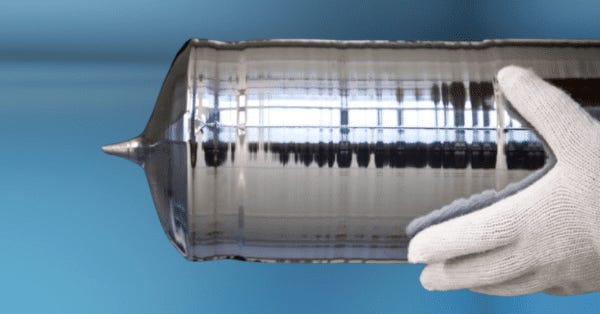
Over several hours you pull a massive cylinder of single-crystal silicon out of the melt. This cylinder is called an ingot.
A typical ingot is about 2 meters long and 300 millimeters in diameter. Some newer fabs are moving to 450mm diameter ingots but those are not widespread yet.
The entire ingot is one perfect crystal. Billions of atoms all lined up in the same direction.
This is the raw material that chips are made from. But we are not done yet.
Slicing Silicon Into Wafers
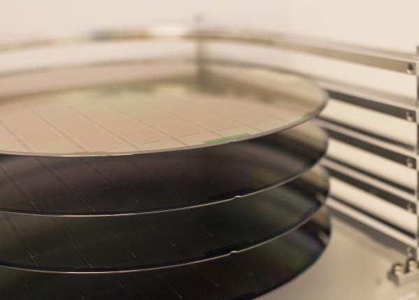
You cannot build chips on a 2-meter-long cylinder of silicon. You need thin flat discs almost like CDs (I hope you’re old enough to remember those).
So the ingot gets sliced into wafers.
First the ingot gets trimmed. The top and bottom get cut off. The sides get ground down to a precise diameter.
Then the ingot goes to a wire saw. This is a machine with a thin wire coated in diamond particles. The wire moves at high speed and slices through the silicon like a slicer cutting meat.
Each slice is incredibly thin. Modern wafers are about 0.75 millimeters thick. Thinner than a credit card. One ingot produces hundreds of wafers.
After slicing the wafers are rough and covered in microscopic damage from the cutting process. So they get polished.
Polishing involves grinding the wafer surface with finer abrasives until it is perfectly smooth and flat.
The final wafer surface is so smooth that if you scaled it up to the size of a big city the tallest bump would be less than a centimeter high.
That level of flatness is required because the circuits built on the wafer are nanometers tall. Any bump or scratch ruins the chip.
Blank silicon wafers ready to be turned into chips. The finished wafers are inspected, cleaned, and packaged for shipment to chip fabs.
Fab stands for Fabrication Facility. These are companies which take the wafers and build the transistors onto each wafer, layer by layer.
TSMC, Samsung, and Intel are some of the most sophisticated fabs out there.
Bigger Wafers = Cheaper Chips
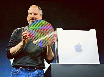
You might have noticed that the industry keeps pushing for bigger wafers. 200mm, 300mm, 450mm.
The reason is pretty simple. Each wafer can hold a certain number of chips depending on the chip size. A bigger wafer holds more chips.
The cost of processing a wafer does not scale with wafer size. Processing a 300mm wafer does not cost twice as much as processing a 200mm wafer even though it has more than twice the area.
So bigger wafers mean more chips per wafer with only a modest increase in processing cost. That drives down the cost per chip.
A 300mm wafer has 2.25 times the area of a 200mm wafer. That means 2.25 times more chips from roughly 1.3 times the processing cost.
The industry has been on 300mm wafers since the early 2000s. The transition to 450mm has been talked about for over a decade but it keeps getting delayed just like GTA 6 :p
The problem is that moving to 450mm requires redesigning every tool in the current fab supply chain. The furnaces, the lithography machines, the deposition tools, everything.
And that is way too expensive and time-consuming.
Just know that the most advanced lithography machines cost around $350 million per unit.
The cost of going to a bigger wafer is in the billions of dollars. And right now the companies can not justify it simply.
So for now 300mm (aka 12 inches) is the standard and will be for the foreseeable future.
What’s Next After Silicon Wafers?
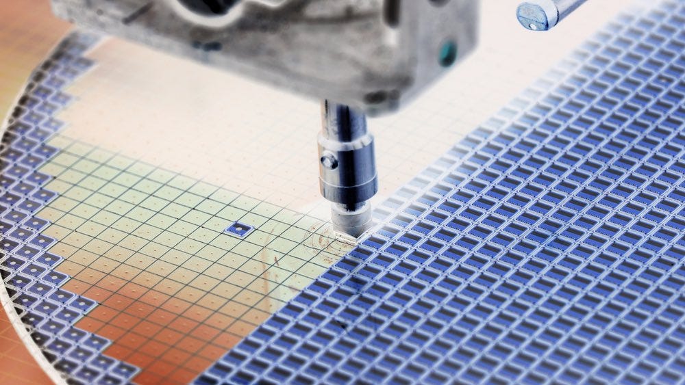
We started with sand on a beach. We ended with a perfectly flat, perfectly pure, single-crystal silicon wafer.
This wafer is the foundation for everything that comes next in the Series.
In the next article we will head into the fab, where those blank wafers get turned into chips with billions of transistors. We will cover lithography (drawing circuits with light), then deposition, etching, and doping, the actual construction of the transistors.
Then in the final article we will cover how chips get tested, cut apart, and packaged, and why some chips cost $50 while others cost $2,000.
But all of that starts here. With sand. The fact that your phone started as sand is not just some analogy I used. It is literally true.
Someone literally mined quartz out of the ground. Someone refined it into polysilicon. Someone grew it into an ingot. And someone sliced it into wafers.
Those wafers traveled to a fab in Taiwan or South Korea where billions of transistors will be built on them.
Then those chips got packaged, tested, and shipped to your phone manufacturer who assembled them into the device you are holding right now.
The entire process from sand to smartphone takes months and involves dozens of companies across multiple countries.
But it all starts with the humble silicon which most people don’t think about when it comes to advanced processors.
I hope this article helped you understand where chips actually come from. The next articles will dive deep into the processes that happen on a wafer.
While writing this article, the exciting thing for me was how simple the chip-making process sounds until you try to dive a bit deep.
Most of us never imagine how complex the process of taking literal sand into polished wafers is.
In the next article, things will get more complex as I go over the transistor side of things.
I would love to know how this newer Series format feels to you guys. Please share any feedback you have down in the comments.


