



Hey there 👋
In the first article of this series, we covered how silicon goes from literal sand to flat wafers.
In the second article, we covered how those wafers get turned into chips with billions of transistors through processes like lithography, etching and doping.
We ended with wafers covered in billions of transistors all connected by microscopic wires.
But those chips are still attached to a giant wafer.
And these chips have not been tested and need to be cut down to size. You cannot just stick a wafer into your phone, right?
So, as the third and last article in this series, this piece will cover the final stages of chip making.
In this article I’ll go over how chips get tested and how they get cut apart and packaged small enough to fit into our smartphones.
If this is your first time reading this article, just know that this is the third in a series of 3 articles on chip making.
It’s best that you go through them in order to know what we’re talking about.
Part 1 is free and open to everyone, so if you are just getting here, start there. Parts 2 and on are for paid subscribers. Both are linked below:


Most Chips Don’t Work on the First Try
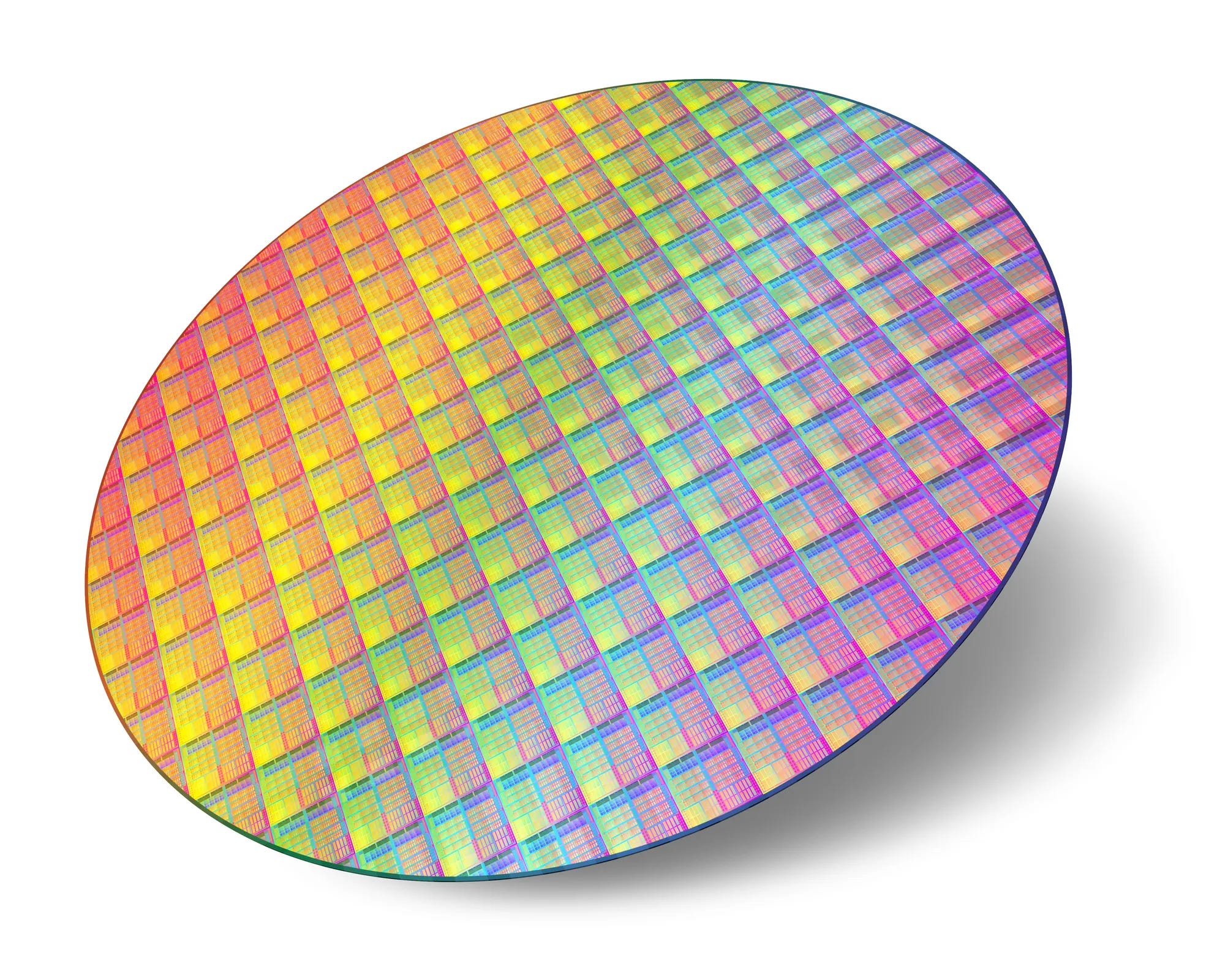
Look, we got through all the processes of creating chips on the wafer but not every chip on a wafer actually works.
In fact many of them do not work at all. They have defects. Transistors that short circuit. Connections that break. Errors that make them useless.
This happens even at the best fabs in the world. Even at TSMC with their cutting-edge processes.
Remember from Part 2 that the chip manufacturing process involves 50 to 100 layers. Each layer requires lithography, deposition, etching, doping.
Every single one of those steps has to be perfect. If any step has even a tiny error the chip fails.
A single speck of dust landing on the wafer during processing can ruin multiple chips. A slight misalignment during lithography ruins chips.
The smaller the transistors the more likely defects become. At 3nm node sizes you are working with features just a few atoms wide.
At that scale everything matters. Temperature variations. Vibrations. Contamination.
So chip manufacturers assume from the start that some percentage of chips will be defective. The question is how many.
This percentage is called yield. And yield determines everything about chip pricing and profitability.
But before we talk about yield we need to understand how fabs figure out which chips work and which do not.