



Hey there 👋
In our previous article in this series, we went through the whole process of mining and purifying silicon to 99.9999999 percent, and all that it takes to create silicon wafers.
Those wafers are perfectly pure, flat, and fully blank. They don’t have any circuits or transistors yet.
Fresh Silicon wafers are somewhat like blank papers. They need someone to write on them to be useful for us in the form of chips.
This article is about exactly that. In this piece we’ll discuss how those blank wafers get turned into chips with billions of working transistors.
The process involves some of the most expensive and precise machines ever built. Light with wavelengths smaller than viruses. Chemistry happening at atomic scales.
And all of it has to be repeated 50 to 100 times to build a single chip.
I’ll try my best to give a full picture of the main processes without drowning you in technical details.
However, you shouldn’t expect this article to be like the regular ones we do here at SK NEXUS.
Saqib here, with one quick side track before you read on.
This week SK NEXUS got its first ever paid subscriber. We went paid only a few weeks ago, and it felt like a gamble. So having someone read our work and decide it’s worth paying for means a lot. To everyone who considered it, and to the one who took the leap, thank you. Really!

Silicon Wafers Arrive at Fab
The blank silicon wafers we covered in our previous article in this series get shipped to a fab.
If you’re unsure about a fab, you may want to check out the previous article in this series.
The fab could be Taiwan’s TSMC, Korea’s Samsung or America’s Intel. These are three of the largest fabs in the world.
These fabs are some of the most expensive buildings ever constructed. A single modern fab costs 20 billion dollars or more to build.
Inside these fabs the air is cleaner than an operating room. A single speck of dust can ruin a chip so the air gets filtered all the time.
Workers wear full body suits called bunny suits. These suits prevent skin cells, hair, or clothing fibers from contaminating the wafers. Just imagine how clean these rooms would be!
The silicon wafers arrive at the fabs in special containers that keep them clean. They get unpacked in cleanrooms where the air is filtered thousands of times per hour.
The real work begins once the wafers land at the fab because fabs are responsible for building billions of transistors on each wafer which are what make a chip.
But before I start nerding about transistors let’s spend a little time trying to understand what a transistor actually is.
What Is a Transistor?
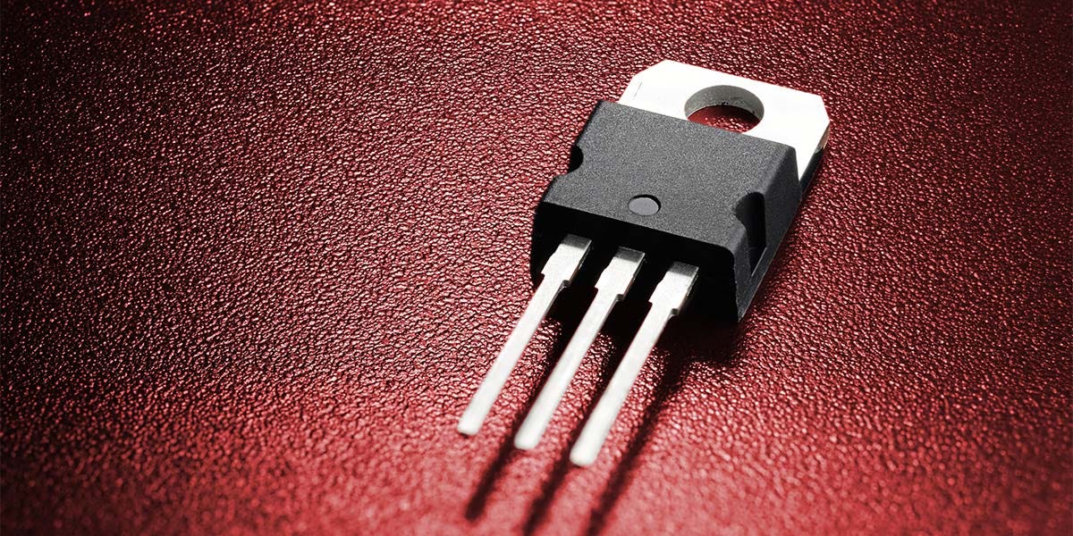
A transistor is actually a switch. It can be on or off. Its purpose is to conduct electricity or block it at any given time.
By turning these switches on and off in specific patterns you get computers to do the work they do.
A modern chip that is in your phone or computer is made of billions of transistors.
And even if you somehow open up your chip, you can’t see transistors with the naked eye. That’s how small they are!
It’s beyond this article to fully cover how transistors allow us to make computers. Maybe, we’ll go through it in a separate article in the future.
On average, a modern phone chip has around 20 billion transistors while your high-end laptop CPU has around 50 billion transistors. All working together to run your apps and games.